 |
| |
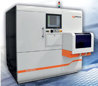
| microDICE™ (TLS-Dicing) - Fast, Clean, and Cost Effective Wafer Dicing |
| |
The microDICE™ laser micromachining system leverages TLS-Dicing™ (thermal laser separation) – a unique technology that uses thermally induced mechanical forces to separate brittle semiconductor materials, such as silicon (Si), silicon carbide (SiC), germanium (Ge) and gallium arsenide (GaAs), into dies with outstanding edge quality while increasing manufacturing yield and throughput. Compared to traditional separation technologies, such as saw dicing and laser ablation, TLS-Dicing™ enables a clean process, micro-crack-free edges, and higher resulting bending strength.
|
| |
Features:
- Significant higher throughput due to dicing speed up to 300 mm/s
- Minimal cost of ownership
- The ability to produce more dies per wafer by reducing street width
|
|
|
Highlights:
| Perfect edge quality of diced chips |
- Nearly no chipping and micro cracks
- Highest bending strength
- Best electrical characteristics
|
| Cost advantages and efficiency |
- High throughput due to high process speed
- Low cost of ownership due to no wear and nearly no consumables
- Zero kerf cleaving with nearly no particle generation
|
|
|
Suited for:
- Semiconductor wafer dicing: Si, SiC, Ge, GaAs
- Thin wafer “TAIKO Cut”
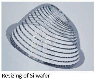
- Wafer resizing
- Wafer cleaving, i.e., Solar Cell half cutting
|
|
| |
 |
|
|